Hacking Roku: Part 3
In the previous post in this series I introduced a test plan for investigating my Roku device. In this installment we’ll cover the first couple of steps.
First, let’s revisit the test plan:
Roku XD Test Plan
Objectives
- Learn basic hardware hacking tools and techniques
- Dump the device firmware
- Get root on the device
Passive Recon
- OSINT / Google
- Inspect exterior
- Disassemble
- Look for useful markings on the PCB
- Identify potentially useful Pins/Headers or test pads
- Look for common groupings or labels that may indicate UART, JTAG, SWD, SPI, etc.
- Identify all ICs
- Locate Data Sheets
- Note any devices that support I2C, SPI, JTAG
Multimeter Testing
- Identify all ground pins/headers/pads with continuity/resistance test
- Identify remaining pins/headers/pads with voltage test
OSINT
One of the first steps in any pentest-type project is to do Open Source Intelligence (OSINT) gathering. Search the web for details about the target such as known vulnerabilities, source code, diagrams, etc. Every bit of information can be helpful.
I found several interesting links:
An old post with some interesting links
A remote code execution (RCE) bug in an older version of the OS
Some Really interesting research from someone who machine-in-the-middle’d the device to get update URLs. Surprisingly, those URLs still work, so I grabbed local copies for later analysis. I’m going to add a new step to my Test Plan:
- Analyze firmware files
Presumably this firmware is much older than the firmware on my device, so will also need to see if perhaps I can figure out where to get a copy of those files.
A complete teardown of a Roku XDS. The XDS was a higher “trim level” than my XD. It has some extra physical ports (Optical Audio, Component Video and 2 USB Ports) but is otherwise physically identical. This article has some great photos of the internal components and even links to some of the relevant data sheets.
This forum thread has some interesting content about modding some of the contemporary Roku devices.
fccid.io - any device with a radio transmitter (bluetooth or wifi, for example) sold in the USA must be registered with the Federal Communications Commission. Subject to some confidentiality, you can find detailed exterior and interior photos and documentation about these devices. While you can find the same content on the official website fcc.gov, you may find it easier to search and view the content on the privately-owned fccid.io . It’s interesting that this device is a “Netgear Roku XD Player.” Perhaps Roku at some point licensed it to Netgear or perhaps Netgear manufactured this early model. The FCCID in this link does not match the one on my device (TC2250X). Searching for that ID reveals what appears to be an identical, non-Netgear branded device: https://fccid.io/TC22050X
Some good information here, and I can mark this item completed on my test plan.
- OSINT / Google
Inspect Exterior
When I started this project I had not given much thought to how I would present/share it with the world, so in the earliest stages of the project I did not take many photos. Fortunately we can refer to the exterior photos here to follow along.
The form factor is a small black box with a square base, rounded corners and rectangular sides. The top is perforated, presumably for ventilation. The front bezel is a translucent red color to allow the LED and iR signals to pass. A cute textile ROKU tag sticks out of one side. On the back is a 5VDC in put, analog stereo audio outputs and analog video output, an RJ45 port for ethernet, and an HDMI output. On the bottom is a label with manufacturer information, MAC addresses for both ethernet and wifi, and the device serial number. A small hole in the lower right corner of the label exposes a reset button.
Finally, hidden under two stickers above the and below the label on the bottom, are the screws that hold the device together.
- Inspect Exterior
Disassemble
Sometimes devices are tricky to disassemble, but the Roku XD is straightforward. Simply remove the two screws on the bottom. It may be necessary to slide something between the upper and lower parts along the back panel above the plugs, but once you have it started, it comes apart easily.
The single board is itself attached to the bottom of the shell with two screws and a retaining clip molded into the front part of the shell. After removing these two screws and gently flexing the clip to free the board it comes away from the shell and now the device is fully disassembled.
- Disassemble
Look for Useful Markings on the PCB
If you are lucky, you might find some obvious markings printed right on the PCB for interfaces such as UART, SWD or JTAG. Alternatively, there may be sets of pins labeled TX, RX, GND, and VCC or 3V3 or 5V for UART. A pin labeled RST might point you toward an SWD or even JTAG interface.
Unfortunately, in the case of the Roku XD … there is really nothing. We will need to do some detective work to see if there are any usable interfaces on the board.
- Look for useful markings on the PCB
Identify potentially useful Pins/Headers or test pads
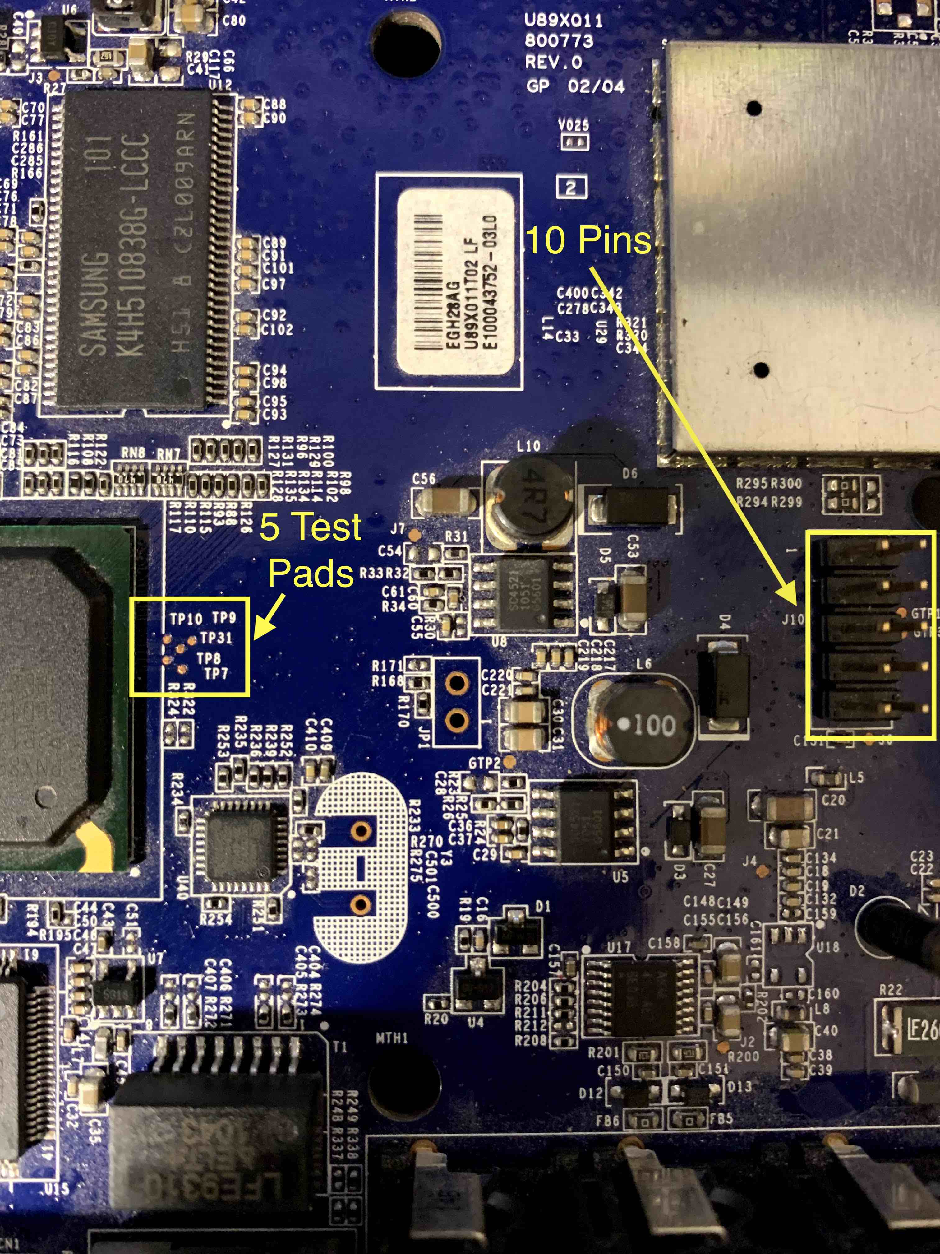
 Next, we’ll inspect the board for anything that we might be able to connect to. On one side of the board is a set of 10 pins. That might be promising. On the opposite side of the board just next to the chip that appears to be the CPU or SoC is a cluster of 5 test pads. JTAG uses up to 5 signals… could a JTAG interface be hidden here?
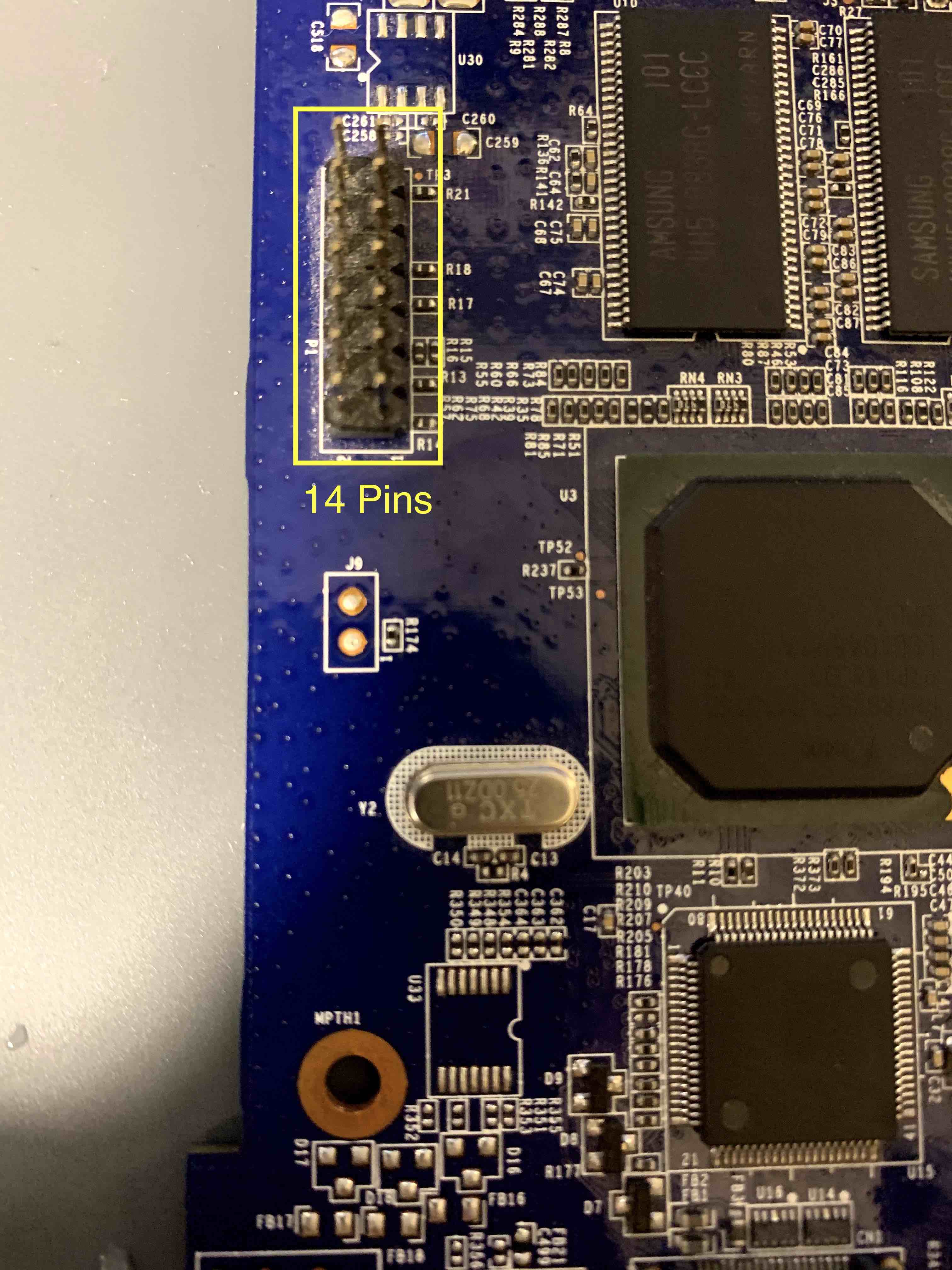
 There is a set of 14 pins on the opposite side of the board. JTAG is often hidden in standard 14-pin headers, so I will want to focus some attention there.
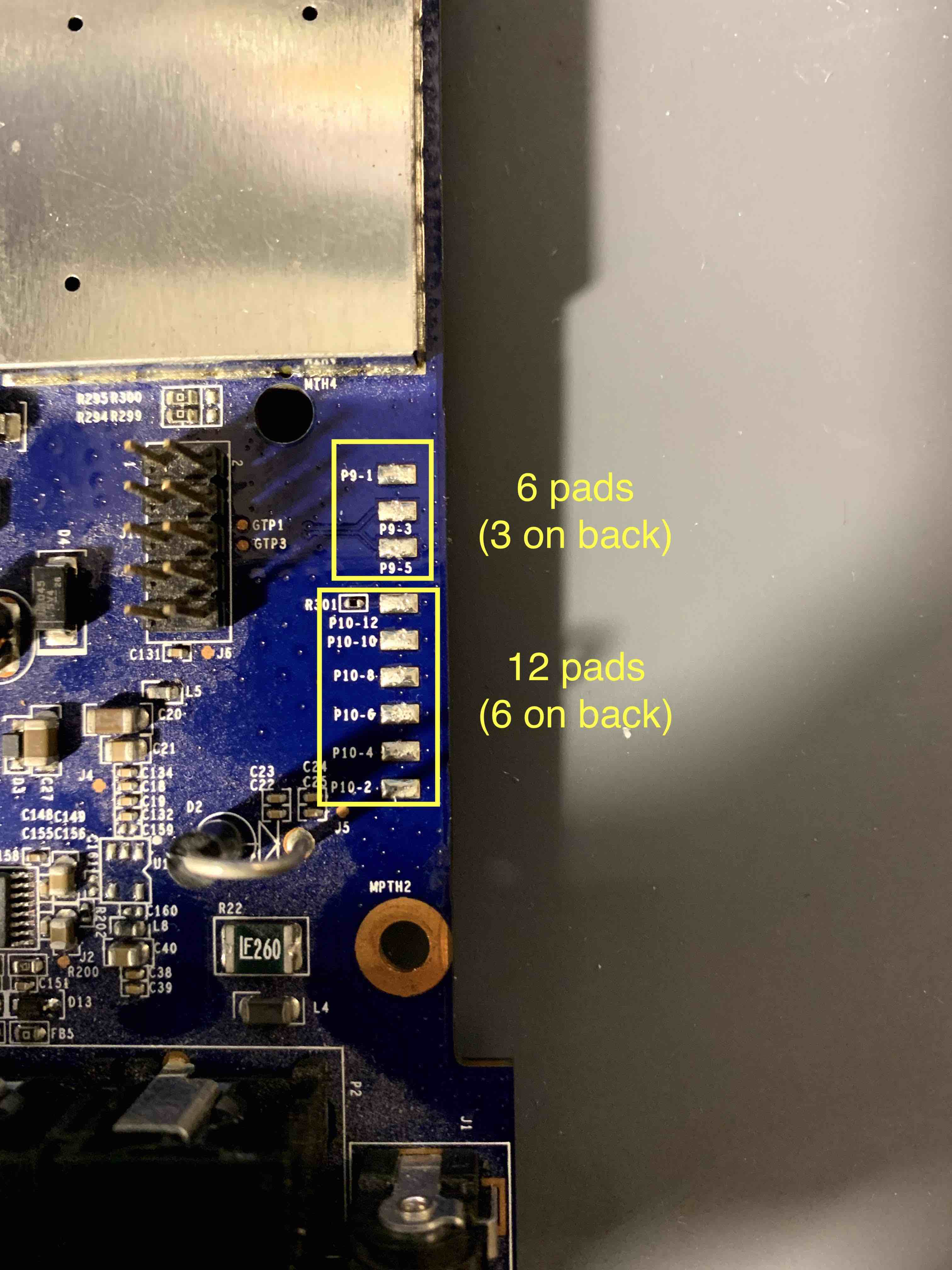
 Finally, next to the 10 pin header in the first image, there is an interesting collection of pads along the edge of the board. Some of them are labeled P9 and some P10 so they appear to be two separate sets. Based on the numbering, there are pads for both sets on both sides of the board, giving us 6 pads for P9 and 12 pads for P10.
Look for common groupings or labels that may indicate UART, JTAG, SWD, SPI, etc.
Unfortunately, there is nothing that is obviously anything anywhere on this board. There are a couple of potential JTAG headers but nothing definite. Actually, because I am doing this specifically to learn hardware hacking techniques, this is not too unfortunate. I am just going to have to learn how to do the detective work necessary to identify any available interfaces!
- Identify potentially useful Pins/Headers or test pads
- Look for common groupings or labels that may indicate UART, JTAG, SWD, SPI, etc.
We’ve knocked off most of our Passive Recon tasks, and we uncovered a new task to analyze the firmware binaries. Here’s how the test plan looks now:
Roku XD Test Plan
Objectives
- Learn basic hardware hacking tools and techniques
- Dump the device firmware
- Get root on the device
Passive Recon
- OSINT / Google
- Inspect exterior
- Disassemble
- Look for useful markings on the PCB
- Identify potentially useful Pins/Headers or test pads
- Look for common groupings or labels that may indicate UART, JTAG, SWD, SPI, etc.
- Identify all ICs
- Locate Data Sheets
- Note any devices that support I2C, SPI, JTAG
Multimeter Testing
- Identify all ground pins/headers/pads with continuity/resistance test
- Identify remaining pins/headers/pads with voltage test
Further Testing
- Analyze firmware files
Coming Up
In Part 4 I will inspect all of the components on the board and maybe even begin trying to identify the pins/pads.