Hacking Roku: Part 4
In this latest installment of my “learn hardware hacking by doing” series, I’ll go over finishing up the initial passive recon phase.
In Part 3 of this series, we did some OSINT, took the Roku XD apart and then examined the PCB for interesting markings and potentially useful pins or pads.
In this post, we’ll try to identify all of the ICs on the board. But first, let’s review the test plan. It’s important to regularly review your test plan to keep track of what has and hasn’t been done. I’ve removed the completed items to reduce clutter; you can always find them on previous posts in this series.
Roku XD Test Plan
Objectives
- Learn basic hardware hacking tools and techniques
- Dump the device firmware
- Get root on the device
Passive Recon
- Identify all ICs
- Locate Data Sheets
- Note any devices that support I2C, SPI, JTAG
Multimeter Testing
- Identify all ground pins/headers/pads with continuity/resistance test
- Identify remaining pins/headers/pads with voltage test
Further Testing
- Analyze firmware files
Identify all ICs
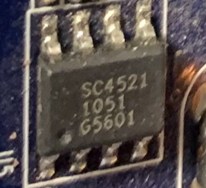
Every IC (Integrated Circuit) on a PCB will be labeled with a part number of some kind and often a manufacturer name. Usually finding key information about what each IC does is as simple as punching the information into a search engine. Not every component on a board is useful from a hacking perspective, however. For example the Roku XD has a couple of SOIC-8 ICs marked SC4521. Serial flash memory sometimes comes in a SOIC-8 package, but a quick search for SC4521 reveals that it is a switching regulator. This probably does not have much value for what we’re trying to learn.
Sometimes the marking on the IC is hard to read. Good lighting and a magnifier or microscope are very helpful. It’s easiest to read the markings if the light hits at an angle. If you really get stuck, rubbing a bit of chalk on the chip and then gently brushing off the excess can fill in the debossed markings and make them more readable.
In practice, I find it easiest to group similar tasks, so I would first collect all of the markings from the ICs and take pictures before searching for data sheets. For the purposes of this post, I’ll list each IC and link to any data sheets I might find.
Here is a tour of the ICs of interest on the Roku XD:
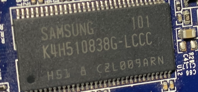
Samsung K4H510838G-LCCC
There are four of these, 2 on the top of the board and 2 on the bottom. These are the RAM chips. Probably not very useful to us.
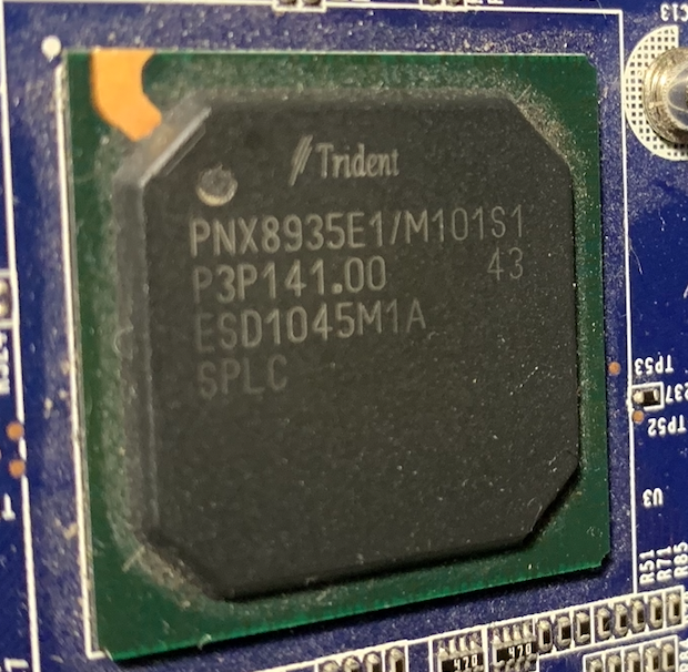
Trident PNX8935E1/M101S1
This is described as a multi-format source decoder. This chip looks like it would be the System-on-Chip (SoC) if the device has one at all. Unfortunately this IC seems to have been produced under a strict NDA. I am unable to find a data sheet or much other information about it at all.
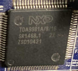
NXP TDA9981A/8/16
HDMI Transmitter. Presumably this is involved with outputting the video stream to HDMI. It sits between the source decoder above and the HDMI port.
According to the data sheet, it does support I2C, which could be useful for us.
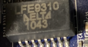
LFE9310
I could not find any information about what this device does.
SC4521
This is the switching regulator that I mentioned above. There are two of these on the Roku.
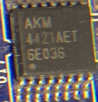
AKM 4421AET
This is a DAC (Digital Analog Converter), presumably used to convert the digital video signals for output via the analog outputs.
This does not have much value for us.
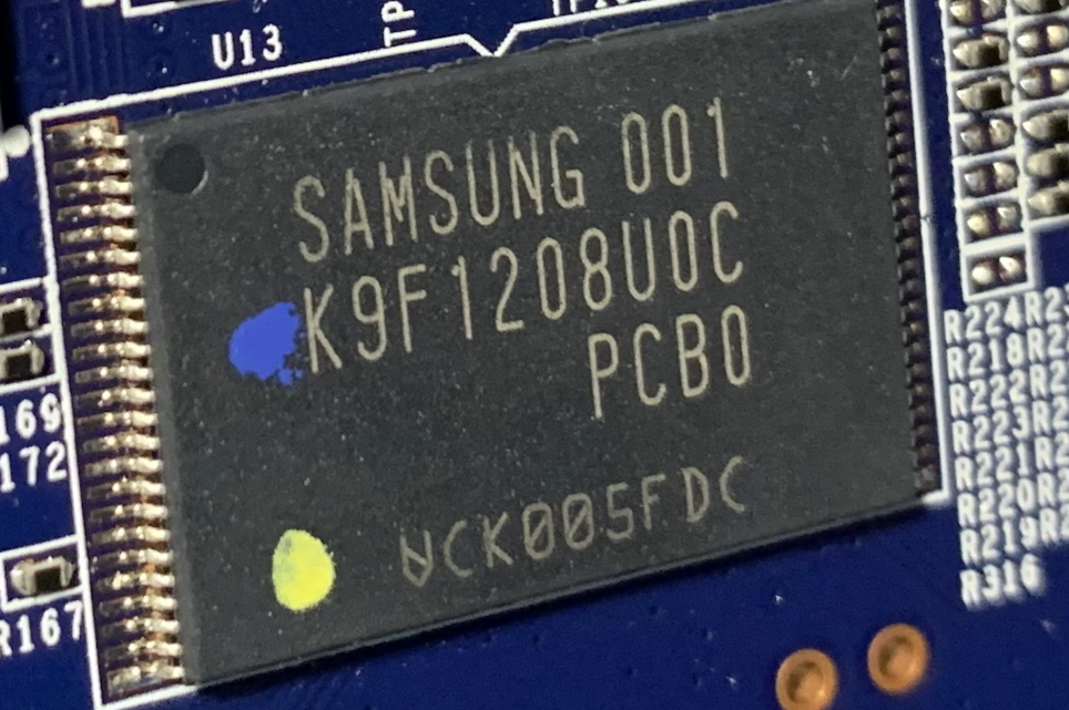
Samsung K9F1208U0C
NAND Flash Memory
This part is of great interest to us. Whatever OS the device has is going to be stored here and other valuable information as well. Accessing the contents of this would complete Objective #2 (Dump Device Firmware). Unfortunately, this kind of chip does not support SPI or I2C, which could make it easier to dump the contents. It may be possible to remove the chip from the board and dump the contents, but that would require some additional equipment that I don’t yet have, and of course, it’s destructive (more on that later). It may also be possible to dump the chip in situ using a clip that goes over top of the chip. This TSOP1 packaging was used on the XBox (among other things) and there are clips available that may work. I would have to source such a clip so I will table that for another time.
I have also seen a pin glitch attack done on this type of memory. While this would not help me access the contents, it could potentially break me out of the bootloader (if I can find a UART to allow me to interact with the board). I’m going to add that to my test plan. Because this is potentially destructive, it should go later in the plan.
- Pin Glitch the NAND Flash chip
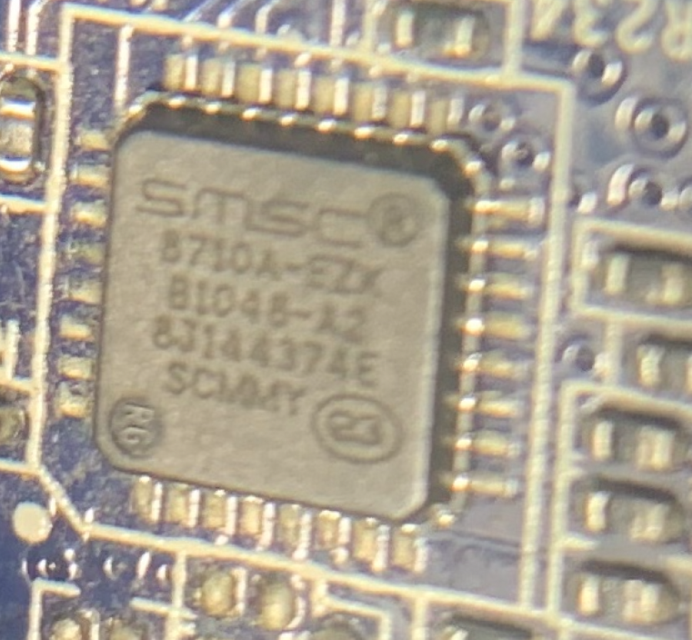
SMSC 8710A-EZX(K?)
This is the ethernet transceiver.
This device supports SMI (Serial Management Interface) which would allow us to control the Ethernet port. It’s interesting but it probably is not very helpful for us.
That covers all of the visible ICs, but there is one place I haven’t checked.
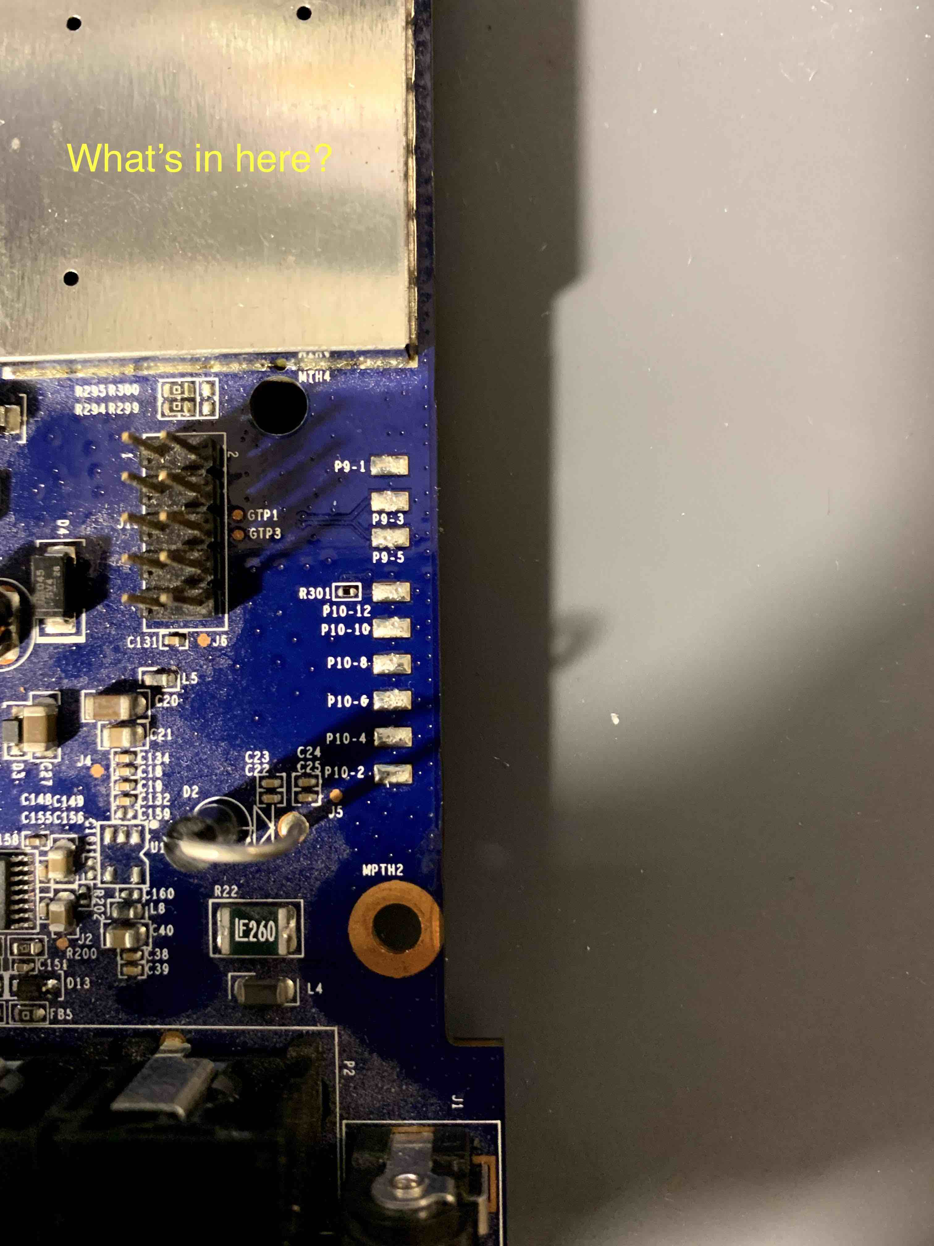
There is a big square shielded block in one corner above the 10-pin header. Based on what we have found and not yet found and the fact that it is shielded, it’s a safe guess that the Wifi transceiver lives under there, but how can we get a look at it?
We could try to remove the shield, but maybe there is a simpler way to get this? In fact, there is. In part 3, we found the FCC submission package at fccid.io. Part of the package is the interior photos where the shield has been removed and we can easily see that the Wifi module is:
Broadcom BCM4323KFBG
I am unable to find a datasheet for this part, but this product brief at least reveals some of the features. Of note, it features an ARM Cortex M3 CPU, which I have seen used to access flash memory via JTAG in other articles. The block diagram also appears to indicate that it supports JTAG which would support that theory.
A word about prioritizing tests
Since hardware hacking has the potential to be destructive, it’s important to weigh the risk of damage to the device when deciding the order of tests. Another consideration is whether backup devices are available. The lowest-risk tests should be carried out first. If I were to try, for example, removing the Flash Memory chip from this device, there’s a good chance that I’ll never get it back to a working state. That’s why my test plan starts with passive recon, followed by multimeter testing which is very low risk as long as you’re careful. Depending on what I do (or do not) find, in the next stage of testing, I’ll add new tests and order them from lowest to highest risk. If backup devices are available, then it’s reasonable to prioritize a high-risk test if it seem promising knowing that you could keep working a replacement device if anything goes wrong. Since the Roku XD was a “target of convenience” that I already had available, I am not too interested in tracking down another one. So, I am going to do my best to do as much work on it as I can before breaking it.
Roku XD Test Plan
Objectives
- Learn basic hardware hacking tools and techniques
- Dump the device firmware
- Get root on the device
Passive Recon
- Identify all ICs
- Locate Data Sheets
- Note any devices that support I2C, SPI, JTAG
Multimeter Testing
- Identify all ground pins/headers/pads with continuity/resistance test
- Identify remaining pins/headers/pads with voltage test
Further Testing
- Analyze firmware files
- Pin Glitch the NAND Flash chip
Looking Ahead
In the next installment we’ll get out the multimeter and start exploring just what all of the pins and pads on this board might do.
